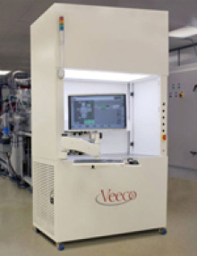
With the help of DOE funding, Veeco is working on reducing epitaxy costs and increasing LED efficiency by developing a physical vapor deposition (PVD) tool for depositing aluminum nitride buffer layers on LED substrates. PVD, also known as "sputtering," is an alternative to metal-organic chemical vapor deposition (MOCVD). PVD is a purely physical process that involves plasma sputter bombardment rather than a chemical reaction at the surface to be coated, as in MOCVD.
PVD can be used on both sapphire and silicon substrates. It could be especially beneficial with silicon, which at the present time poses more problems as an epitaxy substrate than does the widely used but more expensive sapphire. A "greener" process than MOCVD, PVD does not use any toxic chemicals. It also has the potential to use fewer materials. In addition, PVD has the potential for reducing the defect density, which could lead to higher-brightness LEDs.
The objectives of the project are to reduce epitaxy costs by 60 percent due to higher throughput, lower defect density, and reduced yield loss from wafer bow and temperature variations. The next phase of the project will be to prove the manufacturability and cost of ownership, build a high-volume beta tool, and build an LED device. Veeco plans to introduce a production system to the marketplace once the technology has been proven to meet the desired objectives.
Return to Research Highlights

