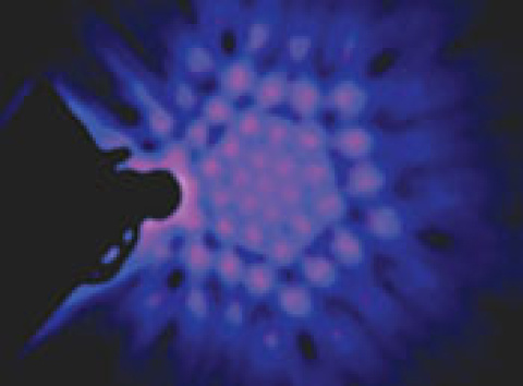
Interferometric Lithography Speeds Process, Enables Larger-Area Pattern
The University of New Mexico (UNM) has been developing interferometric lithography,the use of the interference between a small number of coherent optical beams, to create small-scale periodic patterns in a single, parallel, large-area exposure for this and similar applications. This pattern was written over an area much larger than the final LED (~ 2.5×2.5 cm2 ) in only a few seconds with a pair of two-beam interferometric lithography exposures. The pattern was generated at UNM on a partially fabricated III-Nitride LED wafer. Lumileds Lighting then carried out the remainder of the LED fabrication.
Photonic crystals couple substantially more of the light generated within the active layers of the LED, compared to the light generated with simple planar surfaces. Light output from planar surfaces is limited because of a classical optical effect known as total internal reflection, which allows only a small fraction of the internally generated light to escape from the high refractive-index LED materials. Photonic crystals employ diffractive effects to couple out light that is otherwise unavailable, enhancing the overall efficiency of the LED - an important step towards commercial lighting applications.
Rapid, Inexpensive Pattern Changes are Important for Low-Cost, High Volume Manufacturing
This achievement has both scientific and technological implications. Edge effects in small devices can mask important physics that become evident at larger areas. Large-area devices are important for verifying the extraction efficiency gains available with photonic crystals and for enabling a systematic optimization of the photonic crystal parameters. The interferometric lithography process is very facile, allowing rapid and inexpensive changes in the pattern period, the dimensions of the pattern features, and the pattern symmetry. The interferometric lithography process creates a much larger-area pattern than was used in this experiment, and UNM is already patterning an area of ~ 2.5×2.5 cm2 in a single exposure. Extension to a more engineered, full-wafer patterning tool, necessary for the ultimate goal of low-cost, high-volume manufacturing, is an important future direction.
Return to Research Highlights

